In November 2018, Amazon announced the launch of the inferentia chip during its re: Invent conference. Like any other Amazon innovation, this one had us all hooked. What is so special about this chip?
Designed to process machine learning workloads, Amazon’s inferentia chips claim to have lower latency. This is a pretty big deal, given that the largest semiconductor companies could not do so.
Do you have lots of questions running barefoot in your mind? Well, you are not alone. From Machine Learning engineers to AI scientists to cloud evangelists, everybody has a ton of questions about Amazon Inferentia. So we decided to answer these questions, adding our Patent analysis on the tech. So, let’s unearth what is unique about the architecture of these Inferentia chips.
What is this hype around AWS Inferentia Chip?
The 2018 unveiling of a Custom Machine Learning Inference Chip was a big move for Amazon in the AI domain and a threat to other chip makers.
According to AWS:
AWS Inferentia provides high throughput, low latency inference performance at an extremely low cost. Each chip provides hundreds of TOPS ( terra operations per second) of inference throughput to allow complex models to make fast predictions. For even more performance, multiple AWS Inferentia chips can be used together to drive thousands of TOPS of throughput.
Amazon aims to leave no room for complacency or latency, and AWS Inferentia ensures the services are top-notch.
Why is Amazon making its way into the Chip Industry?
AI-powered products such as Alexa are computation-intensive, requiring a lot of computing power to function. A well-established fact of the domain is that the more computation resources you have, the easier your life becomes.
It looks like Amazon has been preparing to get ahead by developing dedicated, specific-purpose hardware chips that are specifically made to do the computation required in these products.
To get into the depth of why this is a big thing, Let’s first take a look at a few things:
Any machine learning-powered product or service has two essential steps:
- Training, and
- Inference.
Training Phase
In training, a machine is fed to learn the patterns in the given data. This is where the machine gets smarter by learning the complex mathematical function from the data.
Training is often a one-time process, meaning you only have to train a machine once for a specific data set, and then it will be ready for the inference phase.
Inference Phase
The inference phase is where the AI-powered product provides value. In this phase, people use the system for their use cases. This is where the product is actually used, and it’s definitely not a one-time process. In fact, millions of people are using these products at the same time!
For example, consider this: More than 100 million Alexa devices exist. Alexa uses the Inference phase to process millions of user requests. So, the usefulness of Alexa’s system is actually determined by how it operates in the inference phase.
“Compared to GPU-based instances, Inferentia has led to a 25% lower end-to-end latency, and 30% lower cost for Alexa’s text-to-speech(TTS) workloads.”
This is essentially why big tech giants like Google and Amazon are working on such products. For example, in 2016, Google announced its first custom machine learning chip, the Tensor Processing Unit.
Amazon was dependent on Nvidia for chips. AWS CEO Andy Jassy said, ‘GPU makers have focused much on training but too little on inference. So Amazon decided to focus on designing better inference chips.’
A year later, Amazon launched its custom-built processor, Graviton2. In the last couple of years, Amazon has increased the involvement of its own hardware solutions with its services. This move reflects that Amazon is steadily moving towards vertical integration. This is similar to what Apple has been doing with its own silicon efforts.
How did Amazon reach here?
As discussed above, before this release, Amazon had been using the chips made by Nvidia and Intel for its AWS (Amazon Web Services). Amazon felt that despite being really promising, inference chips were not given much attention. So, the company decided to take matters into its own hands.
In 2015, they acquired an Israeli startup, Annapurna Labs, that designs networking chips to help make data centers run more efficiently. They can be said to be Amazon’s brain behind chip design. This was a strategic talent-hiring acquisition to hire inventors like Ron Diamant.
Let’s take a look at the trend of Amazon’s filing in this niche:
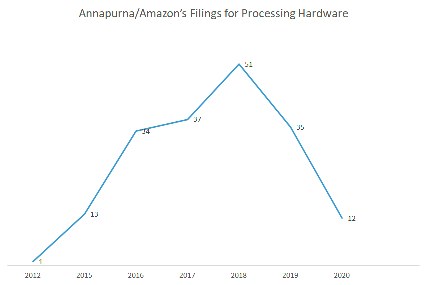
There has been a consistent upward trend for filings that cover some important aspects of Amazon’s chips. Some of the notable innovations:
- Uniform memory access architecture (US10725957B1): This patent discloses a technique to support higher memory capacity without increasing the number of pins on the SoC package or adding complexity to the PCB layout.
- An on-chip hardware performance monitor (US10067847B1) is used to enhance the evaluation of the systems.
- Rate limiting circuit (US10705985B1) for memory interconnects. This rate-limiting circuit reduces retries and removes indeterminate delays, thus lowering transaction latency in the SOC chip.
- On-chip Memory (US10803379B2): This reduces the latency, as seen in the next section.
How did Annapurna solve the problem of latency? What is so special about this chip?
Graphics Processing Units (GPUs) are generally used for training and inference of AI models. They contain multiple computing units optimized for parallel computations. But, as you might already know, GPUs are limited in that they can not share the result from one computation unit and provide it directly to another.
Often, the result must first be written to memory. As machine Learning gets complicated, the ML models grow. Transferring the models in and out of the memory becomes the most crucial task on a system level. Reading from and writing to memory, however, is much slower than the operation of the computation engine. The speed of a neural network can thus be limited by off-chip memory latency. This movement of the model from the computing unit to memory and then back to the computing unit brings high Latency.
So the key here is to reduce this off-chip memory latency. As we have seen above, Amazon has an IP for a chip that contains On-chip memory. This means that the memory is on the same die or in the same package (e.g., the physical enclosure for the die) as the computation matrix. Processors can use this on-chip memory to store intermediate results. In this way, the processor may still be memory-bound, but it may be possible to read the on-chip memory as much as ten or fifty times faster than off-chip memory. Can you imagine what reducing memory delays by this amount can do? It may enable the operation of a neural network to approach the computation speed limit of the processor.
Another thing is the interconnectivity of the chip network (like in US10725957B1). This interconnectivity facilitates moving some computational results from one chip to another without using the memory, thus reducing the latency.
Here is one of the patents Amazon has secured for this:
US10846621B2
The circuit has a memory bank for storing the first set of weight values for a neural network to perform the first task using first input data ( 550) with a known result, where the integrated circuit receives first input data associated with a first task, computes the first result using the first set of weight values and the input data, determines the set of memory banks in an available space during computation of the first result, stores a second set of weight values in the available space, receives second input data associated with a second task and computes a second result using a set of weights ( 506) and the second input data.
How are Semiconductor Giants like Intel and Nvidia falling behind in this?
Now, a question can come. If this technology is superior to what they already have, why don’t Intel/Nvidia do the same?
Well, the biggest obstacle for both companies here is their business model. They provide processors to PC manufacturers and let them assemble the PCs by combining other components such as memory motherboards, graphic cards, etc.
They can make SoC chips that combine multiple hardware components, but each customer will have a different view of what should be on the chip. So, there will be a conflict between Intel, a PC manufacturer, and Microsoft. Since the PC market is still slow due to this shift in chip architectures, Intel/Nvidia is not making such big moves in this direction.
What’s next in the Machine Learning chip domain?
Artificial intelligence and Machine learning have finally become the hottest item on the agendas of the world’s top technology firms, and rightfully so. With the humongous amount of data becoming readily available today, Machine Learning is starting to move to the cloud. Data Scientists will no longer have to custom code or manage infrastructure explicitly. AI and ML will help the systems to scale for them, generate new models on the go, and deliver faster and more accurate results.
“What was deemed impossible a few years ago is not only becoming possible, it’s very quickly becoming necessary and expected.”
-Arvind Krishna, Senior Vice President of Hybrid Cloud and Director of IBM Research.
Tech giants like Google, Facebook, and Twitter are banking on artificial intelligence and machine learning for their future growth. We are closely monitoring the tech development of Machine Learning to the core. In August, Google announced it is moving into chip production with its new Tensor chip for its next-generation Pixel phones. Next, we will examine what is special about Google’s tensor chips and analyze their patent data.
Interested in such analysis? Subscribe to us, and we’ll let you know when our next article goes live.
Or do you have a project where you think we can help? Let’s have a chat:

Authored By: Sukha, Patent Analytics Team


